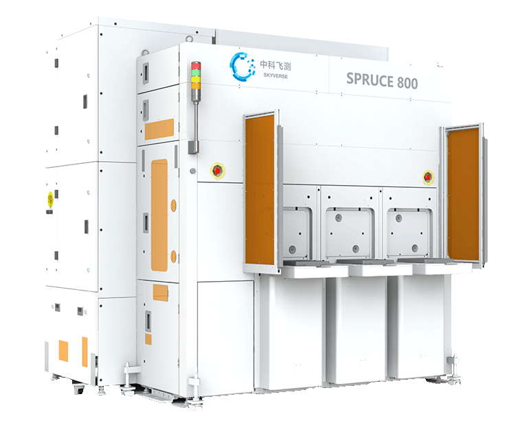
Unpatterned Wafer Defect Inspection Equipment Series

SPRUCE
Home > Products > Equipment Series

Product Introduction

This series of automated equipment is designed to inspect unpatterned wafer, equipped with advanced features for defect counting, spatial distribution analysis, and defect classification. It supports the inspection of different surface types including Bare, Oxide, Nitride, Metal, and more. The equipment employs laser from multiple angles to illuminate the wafer surface. Through the multi-dimensional movement of the sample stage, it achieves a swift and comprehensive scan of the entire sample surface, enabling the precise identification of the defect types and sizes.

Product Features

1、Subjects to SECS/GEM SEMI standards, and is perfectly compatible with factory automation systems.

2、Provides extraordinary reliability.

3、Supports inspection of wafers at multiple design nodes.

4、Covers the demand of IC factories, wafer factories, and semiconductor equipment factories.

5、Applies to wafers of 2-12 inches, III-V compound semiconductors inclusive.

Previous Product

Null